- 您现在的位置:买卖IC网 > Sheet目录3841 > PIC18F67K22-I/PTRSL (Microchip Technology)MCU PIC 128K FLASH XLP 64TQFP
P89V52X2_3
NXP B.V. 2009. All rights reserved.
Product data sheet
Rev. 03 — 4 May 2009
46 of 57
NXP Semiconductors
P89V52X2
80C51 with 256 B RAM, 192 B data EEPROM
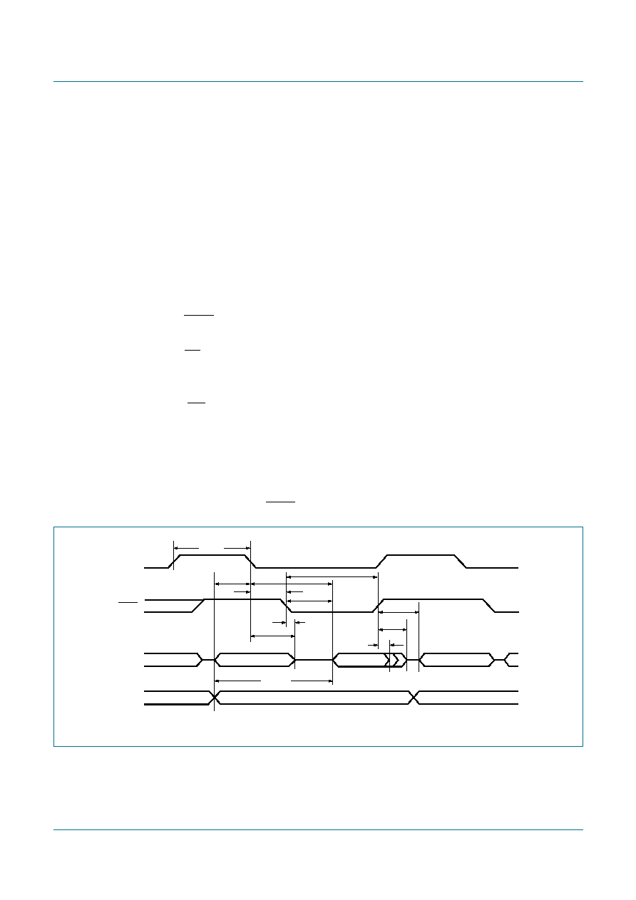
9.1 Explanation of symbols
Each timing symbol has 5 characters. The rst character is always a ‘t’ (stands for time).
The other characters, depending on their positions, stand for the name of a signal or the
logical status of that signal. The following is a list of all the characters and what they stand
for.
A — Address
C — Clock
D — Input data
H — Logic level HIGH
I — Instruction (program memory contents)
L — Logic level LOW or ALE
P — PSEN
Q — Output data
R — RD signal
T — Time
V — Valid
W — WR signal
X — No longer a valid logic level
Z — High impedance (Float)
Example:
tAVLL = Address valid to ALE LOW time
tLLPL = ALE LOW to PSEN LOW time
Fig 21. External program memory read cycle
002aaa548
port 2
PSEN
ALE
A0 to A7
tLLAX
tPLAZ
tPXIZ
tLLPL
tAVIV
tAVLL
tLLIV
tPLIV
tPLPH
INSTR IN
A8 to A15
A0 to A7
port 0
tPXIX
tPXAV
tLHLL
发布紧急采购,3分钟左右您将得到回复。
相关PDF资料
PIC18F66K90-I/MRRSL
MCU PIC 64K FLASH MEM XLP 64QFN
PIC16LC621-04/SO
IC MCU OTP 1KX14 COMP 18SOIC
PIC18LF2410-I/SP
IC MCU FLASH 8KX16 28-DIP
DSPIC30F3013-20I/SP
IC DSPIC MCU/DSP 24K 28DIP
PIC18LF6390-I/PT
IC PIC MCU FLASH 4KX16 64TQFP
DSPIC30F3013-30I/SP
IC DSPIC MCU/DSP 24K 28DIP
DSPIC33FJ32MC202-E/SO
IC DSPIC MCU/DSP 32K 28SOIC
52745-0896
CONN FFC 8POS .5MM R/A ZIF SMD
相关代理商/技术参数
PIC18F67K22-I/PTRSL
制造商:Microchip Technology Inc 功能描述:IC 8BIT MCU PIC18F 16MIPS 制造商:Microchip Technology Inc 功能描述:IC, 8BIT MCU, PIC18F, 16MIPS, TQFP-64
PIC18F67K22T-I/MR
功能描述:8位微控制器 -MCU 128kB Flash 4kB RAM
RoHS:否 制造商:Silicon Labs 核心:8051 处理器系列:C8051F39x 数据总线宽度:8 bit 最大时钟频率:50 MHz 程序存储器大小:16 KB 数据 RAM 大小:1 KB 片上 ADC:Yes 工作电源电压:1.8 V to 3.6 V 工作温度范围:- 40 C to + 105 C 封装 / 箱体:QFN-20 安装风格:SMD/SMT
PIC18F67K22T-I/MRRSL
功能描述:8位微控制器 -MCU 128KB Flash 4KB RAM nanoWatt XLP GP RoHS:否 制造商:Silicon Labs 核心:8051 处理器系列:C8051F39x 数据总线宽度:8 bit 最大时钟频率:50 MHz 程序存储器大小:16 KB 数据 RAM 大小:1 KB 片上 ADC:Yes 工作电源电压:1.8 V to 3.6 V 工作温度范围:- 40 C to + 105 C 封装 / 箱体:QFN-20 安装风格:SMD/SMT
PIC18F67K22T-I/PT
功能描述:8位微控制器 -MCU 128kB Flash 4kB RAM
RoHS:否 制造商:Silicon Labs 核心:8051 处理器系列:C8051F39x 数据总线宽度:8 bit 最大时钟频率:50 MHz 程序存储器大小:16 KB 数据 RAM 大小:1 KB 片上 ADC:Yes 工作电源电压:1.8 V to 3.6 V 工作温度范围:- 40 C to + 105 C 封装 / 箱体:QFN-20 安装风格:SMD/SMT
PIC18F67K22T-I/PTRSL
功能描述:8位微控制器 -MCU 128KB Flash 4KB RAM nanoWatt XLP GP RoHS:否 制造商:Silicon Labs 核心:8051 处理器系列:C8051F39x 数据总线宽度:8 bit 最大时钟频率:50 MHz 程序存储器大小:16 KB 数据 RAM 大小:1 KB 片上 ADC:Yes 工作电源电压:1.8 V to 3.6 V 工作温度范围:- 40 C to + 105 C 封装 / 箱体:QFN-20 安装风格:SMD/SMT
PIC18F67K90-E/MR
功能描述:8位微控制器 -MCU 128KB Flash 4KB RAM LCD
RoHS:否 制造商:Silicon Labs 核心:8051 处理器系列:C8051F39x 数据总线宽度:8 bit 最大时钟频率:50 MHz 程序存储器大小:16 KB 数据 RAM 大小:1 KB 片上 ADC:Yes 工作电源电压:1.8 V to 3.6 V 工作温度范围:- 40 C to + 105 C 封装 / 箱体:QFN-20 安装风格:SMD/SMT
PIC18F67K90-E/PT
功能描述:8位微控制器 -MCU 128KB Flash 4KB RAM LCD
RoHS:否 制造商:Silicon Labs 核心:8051 处理器系列:C8051F39x 数据总线宽度:8 bit 最大时钟频率:50 MHz 程序存储器大小:16 KB 数据 RAM 大小:1 KB 片上 ADC:Yes 工作电源电压:1.8 V to 3.6 V 工作温度范围:- 40 C to + 105 C 封装 / 箱体:QFN-20 安装风格:SMD/SMT
PIC18F67K90-I/MR
功能描述:8位微控制器 -MCU 128kB Flash 4kB RAM LCD
RoHS:否 制造商:Silicon Labs 核心:8051 处理器系列:C8051F39x 数据总线宽度:8 bit 最大时钟频率:50 MHz 程序存储器大小:16 KB 数据 RAM 大小:1 KB 片上 ADC:Yes 工作电源电压:1.8 V to 3.6 V 工作温度范围:- 40 C to + 105 C 封装 / 箱体:QFN-20 安装风格:SMD/SMT